GATE question papers: Electronics and Communication Engineering 2008 (EC)
Q. 1 to 20 Carry One Mark Each
1. All the four entries of the 2×2 matrix p =  are
nonzero, and one of its eigenvalues is zero. Which of the following statements
is true?
are
nonzero, and one of its eigenvalues is zero. Which of the following statements
is true?
(A) p11 p22 - p12 p21 = 1 (B) p11
p22 - p12 p21
= -1
(C) p11 p220 - p12 p21 = 0 (D) p11
p22 + p12 p21 = 0
2. The system of linear equations
4x + 2y = 7
2x + y = 6
has
(A) a unique solution (B) no
solution
(C) an infinite number of solutions (D) exactly
two distinct solutions
3. The equation sin (z) = 10has
(A) no real or complex solution (B) exactly
two distinct complex solutions
(C) a unique solution (D) an
infinite number of complex solutions
4. For real values of x, the minimum value of the
function f (x) = exp (x) + exp (-x) is
(A) 2 (B) 1
(C) 0.5 (D) 0
5. Which of the following functions would have
only odd powers of x in its Taylor series expansion about the point x=0?
(A) (3) sin x (B) (2)
sin x (C) (3) cos x (D) (2) cos x
6. Which of the following is a solution to the
differential equation 
(A) x( t)
= 3e-t (B) x(
t) = 3e-3t (C) x(
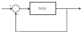
t) =  (D) x(
t) = 3t2
(D) x(
t) = 3t2
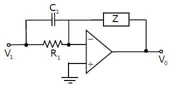
7. In the following graph, the number of trees
(P) and the number of cut-sets (Q) are
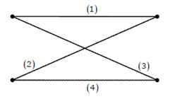
(A) P=2, Q=2
(B) P=2, Q=6
(C) P=4, Q=6
(D) P=4, Q=10
8.
In the following circuit, the switch S is closed at t=0. The rate of
change of current  is
given by
is
given by
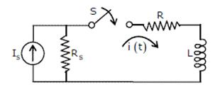
(A) 0
(B) 
(C) 
(D) ¥
9. The input and output of a continuous time
system are respectively denoted by x(t) and y(t). Which of the following
descriptions corresponds to a causal system?
(A) y (t) = x (t - 2) + x (t + 4) (B) y
(t) = (t - 4) x (t
+ 1)
(C) y (t) = (t + 4) x
(t - 1) (D) y
(t) = (t + 5) x (t + 5)
10. The impulse response h (t) of a linear
time-invariant continuous time system is described by h(t) = exp (at)u(t) + exp (bt)u(-t), where u(t) denotes the unit step function,
and a and b are real constants. This system is stable if
(A) a
is positive and b is positive (B) a is negative and b is negative
(C) a
is positive and b is negative (D) a is negative and b is positive
11. The pole-zero plot given below corresponds to
a
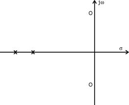
(A) Low pass filter (B) High
pass filter
(C) Band pass filter (D) Notch
filter
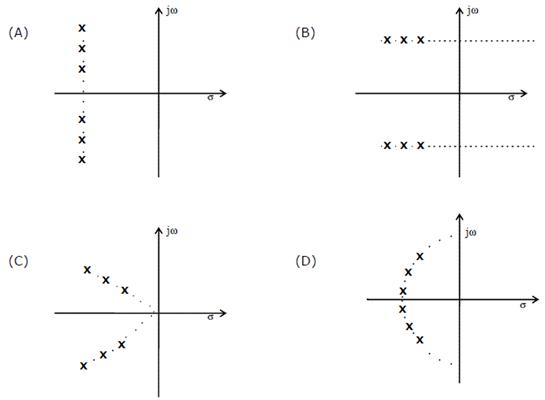
12. Step responses of a set of three second-order
underdamped systems all have the same percentage overshoot. Which of the
following diagrams represents the poles of the three systems?
13. Which of the following is NOT associated with
a p-n junction?
(A) Junction capacitance (B) Charge
Storage Capacitance
(C) Depletion Capacitance (D) Channel
Length Modulation
14. Which of the following is true?
(A) A silicon wafer heavily doped
with boron is a p+ substrate
(B) A silicon wafer lightly doped
with boron is a p+ substrate
(C) A silicon wafer heavily doped
with arsenic is a p+ substrate
(D) A silicon wafer lightly doped
with arsenic is a p+ substrate
15. For a Hertz dipole antenna, the half power
beam width (HPBW) in the E-plane is
(A) 360°
(B) 180° (C) 90° (D) 45°
16. For static electric and magnetic fields in an
inhomogeneous source-free medium, which of the following represents the correct
form of two of Maxwell's equations?
(A)  (B)
(B)  (C)
(C)  (D)
(D) 
17. In the following limiter circuit, an input
voltage Vi = 10sin100pt
applied. Assume that the diode drop is 0.7V when it is forward biased. The
Zener breakdown voltage is 6.8V.
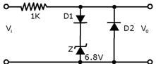
The maximum and minimum values of the output
voltage respectively are
(A) 6.1V, - 0.7V (B) 0.7V, -
7.5V (C) 7.5V, - 0.7V (D) 7.5V,
- 7.5V
18. A silicon wafer has 100nm of oxide on it and
is inserted in a furnace at a temperature above 1000°C for further oxidation in dry oxygen. The oxidation rate
(A) is independent of current oxide
thickness and temperature
(B) is independent of current oxide
thickness but depends on temperature
(C) slows down as the oxide grows
(D) is zero as the existing oxide
prevents further oxidation
19. The drain current of a MOSFET in saturation
is given by 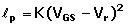 where K is a constant. The
magnitude of the transconductance gm is
where K is a constant. The
magnitude of the transconductance gm is
(A)  (B) 2K(VGS
- VT) (C)
(B) 2K(VGS
- VT) (C)  (D)
(D) 
20. Consider the amplitude modulated (AM) signal
Ac cos wc t +
2cos wm t cos wc t. For demodulating the signal
using envelope detector, the minimum value of Ac should be
(A) 2 (B) 1
(C) 0.5 (D) 0
Q. 21 to 75 carry two Marks Each
21. The Thevenin equivalent impedance Zth
between the nodes P and Q in the following circuit is
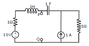
(A) 1 (B) 1
+ s + (C) 2
+ s + (D)
(C) 2
+ s + (D) 
22. The driving point impedance of the following
network
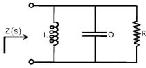
is given by Z (s ) = .
The component values are
.
The component values are
(A) L = 5H, R = 0.5Ω, C = 0.1F (B) L = 0.1H,
R = 0.5 Ω, C = 5F
(C) L = 5H, R = 2 Ω, C = 0.1F (D) L =
0.1H, R = 2 Ω, C = 5F
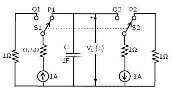
23. The circuit shown in the figure is used to
charge the capacitor C alternately from two current sources as indicated. The
switches S1 and S2 are mechanically coupled and connected as follows
For 2nT £
t < (2n + 1) T, (n = 0, 1,
2 ...) S1 to P1 and S2 to P2
Assume that the capacitor has zero initial
charge. Given that u (t) is a unit step function, the voltage Vc (t)
across the capacitor is given be
(A)  (B) u
(t) + 2
(B) u
(t) + 2
(C) tu(t) + 2 (D)
(D) 
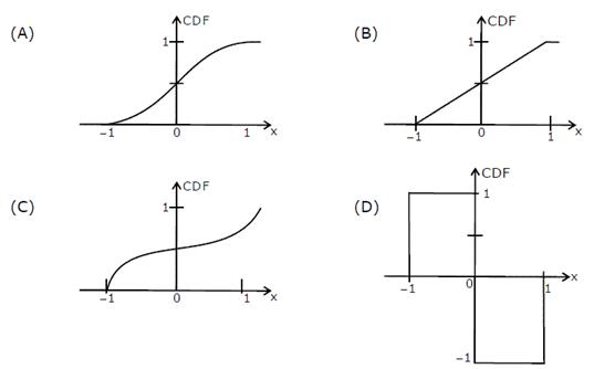
24. The probability density function (PDF) of a
random variable X is as shown below
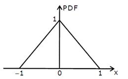
The corresponding cumulative distribution
function (CDF) has the form
25. The recursion relation to solve x=e-x using Newton Raphson method is
(A) xn+1 =  (B) xn+1
= xn -
(B) xn+1
= xn -
(C) xn+1 = (1 + x n) (D) xn+1
=
(D) xn+1
= 
26. The residue of the function f(z) =  at
z = 2 is
at
z = 2 is
(A)  (B)
(B)  (C)
(C)  (D)
(D) 
27. Consider the matrix p =  The
value of ep is
The
value of ep is
(A)  (B)
(B) 
(C)  (D)
(D) 
28. In the Taylor series expansion of exp(x) + sin(x)
about the point x=p, the coefficient of
(x - p
)2 is
(A) exp(p) (B) 0.5exp (p) (C) exp (p)
+ 1 (D) exp (p) - 1
29. Px (x) = M exp (-2 |x| ) + Nexp (-3 |x| ) is the probability density function for the real random
variable X, over the entire x axis. M and N are both positive real numbers. The
equation relating M and N is
(A) M +  N
= 1 (B) 2M +
N
= 1 (B) 2M +  N
= 1 (C) M + N = 1 (D) M + N = 3
N
= 1 (C) M + N = 1 (D) M + N = 3
30. The value of the integral of the function g(x,
y) = 4x3 + 10y4 along the straight line segment from
the point (0, 0) to the point (1, 2) in the x-y plane is
(A) 33 (B) 35
(C) 40 (D) 56
31. A linear, time-invariant, causal continuous
time system has a rational transfer function with simple poles at s=-2 and
s=-4, and one simple zero at s=-1. A unit step u(t) is applied at the input of
the system. At steady state, the output has constant value of 1. The impulse
response of this system is
(A) [exp (-2t) + exp (-4t)] u(t)
(B) [-4exp
(-2t) + 12 exp (-4t) - exp (-t)] u(t)
(C) [-4exp
(-2t) + 12 exp (-4t)] u(t)
(D) [-0.5exp
(-2t) + 1.5exp (-4t)] u(t)
32. The signal x(t) is described by
x(t) = 
Two of the angular frequencies at which its
Fourier transform becomes zero are
(A) p,
2p (B) 0.5p, 1.5p
(C) 0, p (D) 2p, 2.5p
33. A discrete time linear shift-invariant system
has an impulse response h[n] with h[0]=1, h[1]=-1. h[2]-2, and zero otherwise.
The system is given an input sequence x[n] with x[0] x[2] -1, and zero
otherwise. The number of nonzero samples in the output sequence y[n], and the
value of y[2] are, respectively
(A) 5, 2 (B) 6,
2 (C) 6, 1 (D) 5, 3
34. Consider points P and Q in the x-y plane,
with P = (1, 0) and Q = (0, 1). The line integral 
 along
the semicircle with the line segment PQ as its diameter
along
the semicircle with the line segment PQ as its diameter
(A) is -1
(B) is 0
(C) is 1
(D) depends on the direction
(clockwise or anti-clockwise) of the semicircle
35. Let x(t) be the input and y(t) be the output
of a continuous time system. Match the system properties P1, P2 and P3 with
system relations R1, R2, R3, R4.
Properties Relations
P1: Linear but NOT time-invariant R1:
y (t) = t2 x (t)
P2: Time-invariant but NOT linear R2:
y (t) = t |x (t)|
P3: Linear and time-invariant R3:
y (t) = |x (t)|
R4:
y (t) = x (t - 5)
(A) (P1, R1), (P2, R3), (P3, R4) (B) (P1,
R2), (P2, R3), (P3, R4)
(C) (P1, R3), (P2, R1), (P3, R2) (D) (P1,
R1), (P2, R2), (P3, R3)
36. A memoryless source emits n symbols each with
a probability p. The entropy of the source as a function of n
(A) increases as log n (B) decreases
as log (1/n)
(C) increases as n (D) increases
as n log n
37. {x(n)} is a real-valued periodic sequence
with a period N. x(n) and X(k) form Npoint. Discrete Fourier Transform (DFT)
pairs. The DFT Y (k) of the sequence
y(n) = 
(A) |x (k)|2 (B) 
(C)  (D) 0
(D) 0
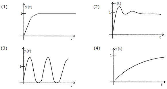
38. Group I lists a set of four transfer
functions. Group II gives a list of possible step responses y(t). Match the
step responses with the corresponding transfer functions
Group I
p =  Q
=
Q
=  R
=
R
=  S
=
S
= 
Group II
(A) P-3, Q-1, R-4, S-2 (B) P-3,
Q-2, R-4, S-1
(C) P-2, Q-1, R-4, S-3 (D) P-3,
Q-4, R-1, S-2
39. A certain system has transfer function G(s) = a is a parameter. Consider the standard
negative unity feedback configuration as shown below
a is a parameter. Consider the standard
negative unity feedback configuration as shown below
Which of the following statements is true?
(A) The closed loop system in never
stable for any value of a
(B) For some positive values of a,
the closed loop system is stable, but not for all positive values
(C) For all positive values of a, the
closed loop system is stable
(D) The closed loop system is stable
for all values of a, both positive and negative
40. A single flow graph of a system is given
below
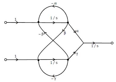
The set of equations that correspond to this
signal flow graph is
(A) 
(B) 
(C) 
(D) 
41. The number of open right half plane poles of G(s)
 is
is
(A) 0 (B) 1
(C) 2 (D) 3
42. The magnitude of frequency response of an
underdamped second order system is 5 at 0rad/sec and peaks to The
transfer function of the system is
The
transfer function of the system is
(A)  (B)
(B) 
(C)  (D)
(D) 
43. Group 1 gives two possible choices for the
impedance Z in the diagram. The circuit elements in Z satisfy the condition R2
C2 >R1 C1. The transfer function  represents
a kind of controller. Match the impedances in Group I with the types of
controllers in Group II.
represents
a kind of controller. Match the impedances in Group I with the types of
controllers in Group II.
Group I Group
II
P. 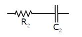 1.
PID controller
1.
PID controller
2.
Lead compensator
3.
Lag compensator
Q. 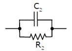
(A) Q -
1,R - 2 (B) Q - 1,R -
3 (C) Q - 2,R - 3 (D) Q - 3,R -
2
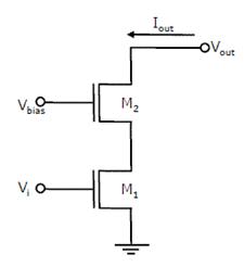
44. For the circuit shown in the following
figure, transistors M1 and M2 are identical NMOS transistors. Assume that M2 is
in saturation and the output is unloaded
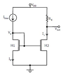
The current Ix is related to Ibias
as
(A) Ix = Ibias
+ Is (B) Ix
= Ibias
(C) Ix = Ibias - Is (D) Ix
= Ibias -
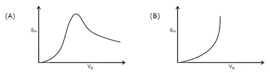
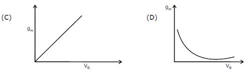
45. The measured transconductance gm
of an NMOS transistor operating in the linear region is plotted against the
gate voltage VG at constant drain voltage VD. Which of
the following figures represents the expected dependence of gm on VG?
46. Consider the following circuit using an ideal
OPAMP. The I-V characteristics of the diode is described by the relation I = Io where VT = 25mV, I0 = 1mA
and V is the voltage across the diode (taken as positive for forward bias).
where VT = 25mV, I0 = 1mA
and V is the voltage across the diode (taken as positive for forward bias).
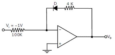
For an input voltage V1 = -1V, the output voltage V0 is
(A) 0 V (B) 0.1V
(C) 0.7V 3(D) 1.1V
47.
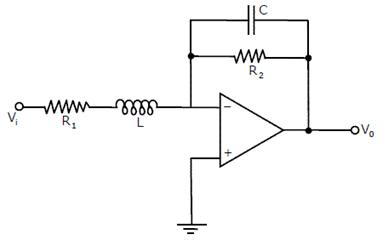
The OPAMP circuit shown above represents a
(A) high pass filter (B) low
pass filter
(C) band pass filter (D) band
reject filter
48. Two identical
NMOS transistors M1 and M2 are connected as shown below. Vbias is chosen
so that both transistors are in saturation. The equivalent gm of the
pair is defined to be  at
constant Vout.
at
constant Vout.
The equivalent gm's of the pair
is
(A) The sum of individual gm's
of the transistors
(B) The product of individual gm's
of the transistors
(C) Nearly equal to the gm
of M1
(D) Nearly equal to gm /g0
of M2
49. An 8085 executes the following instructions
2710 LXI H, 30A0H
2713 DAD H
2714 PCHL
All addresses and constants are in Hex. Let
PC be the contents of the program counter and HL be the contents of the HL
register pair just after executing PCHL.
Which of the following statements is correct
(A) PC = 2715H (B) PC =
30A0H (C) PC = 6140H (D) PC = 6140H
HL = 30A0H HL
= 2715H HL = 6140H HL = 2715H
50. An astable multivibrator circuit using IC 555
timer is shown below. Assume that the circuit is oscillating steadily
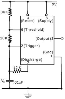
The voltage Vc across the
capacitor varies between
(A) 3V to 5V (B) 3V
to 6V (C) 3.6V to 6V (D) 3.6V to 5V
51. Silicon is doped with boron to a
concentration of 4×10¹⁷
atoms/cm3. Assuming the
intrinsic carrier concentration of silicon to be 1.5×10¹⁰/cm3 and the value of to be 25mV at 300K
Compared to undoped silicon, the Fermi level
of doped silicon
(A) Goes down by 0.13eV (B) Goes
up by 0.13eV
(C) Goes down by 0.427eV (D) Goes
up by 0.427eV
52.
The cross section of a JFET is shown in the following figure. Let Va
be -2V and let Vp be the initial pinch-off voltage. If the width W
is doubled (with other geometrical parameters and doping levels remaining the
same), then the ratio between the mutual transconductances of the initial and
the modified JFET is
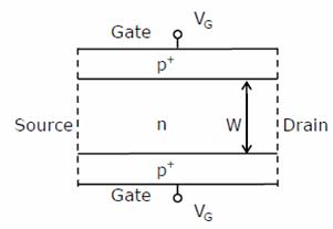
(A) 4 (B) 
(C)  (D)
(D) 
53. Consider the Schmidt trigger circuit shown
below.
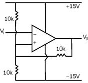
A triangular wave which goes from -12V to
12V is applied to the inverting input of the OPAMP. Assume that the output of
the OPAMP sings from +15V to -15V. The voltage at the non-inverting input
switches between
(A) -12V and +12V (B) -7.5V
and +7.5V (C) -5V and +5V (D) 0V and 5V
54. The logic function implemented by the
following circuit at the terminal OUT is
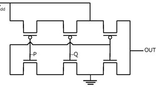
(A) P NOR Q (B) P
NAND Q (C) P OR Q (D) P AND Q
55. Consider the following assertions
S1: For Zener effect to occur, a very abrupt
junction is required
S2: For quantum tunneling to occur, a very
narrow energy barrier is required
Which of the following is correct?
(A) Only S2 is true
(B) S1 and S2 are both true but S2 is
not a reason for S1
(C) S1 and S2 are both true and S2 is
a reason for S1
(D) Both S1 and S2 are false
56. The two numbers represented in signed 2's
complement form are P = 11101101 and Q = 11100110. If Q is subtracted from P,
the value obtained in signed 2's complement form is
(A) 100000111 (B) 00000111
(C) 11111001 (D) 111111001
57. Which of the following Boolean Expression
correctly represents the relation between P, Q, R and M1?
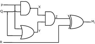
(A) M1 = (P OR Q) XOR R
(B) M1 = (P AND Q) XOR R
(C) M1 = (P NOR Q) XOR R
(D) M1 = (P XOR Q) XOR R
58. For the circuit shown in the following figure
I0-I3 are inputs to the 4:1 multiplexer R(MSB) and S are
control bits
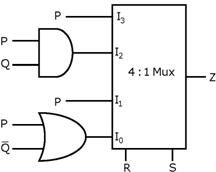
The output Z can be represented by
(A) PQ + P S
+
S
+ 
(B) P
+ PQ +
+ 
(C)  +
+  QR
+ PQRS +
QR
+ PQRS +
(D) PQ
+ PQR + PQS
+
+ PQS
+
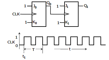
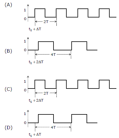
59. For each of the positive edge-triggered J-K
flip flop used in the following figure, the propagation delay is DT
Which of the following waveforms correctly
represents the output at Q1?
60. For the circuit shown in the figure, D has a
transition from 0 to 1 after CLK changes from 1 to 0. Assume gate delays to be
negligible
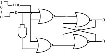
Which of the following statements is true?
(A) Q goes to 1 at the CLK transition
and stays at 1
(B) Q goes to 0 at the CLK transition
and stays at 0
(C) Q goes to 1 at the CLK transition
and goes to 0 when D goes to 1
(D) Q goes to 0 at the CLK transition
and goes to 1 when D goes to 1
61. A rectangular waveguide of internal
dimensions (a = 4cm and b = 3) is to be operated in TE11 mode. The
minimum operating frequency is
(A) 6.25GHz (B) 6.0GHz
(C) 5.0GHz (D) 3.75GHz
62. One of a loss-less transmission line having
the characteristic impedance of 75Ω and
length of 1cm is short-circuited. At 3GHz, the input impedance at the other end
of the transmission line is
(A) 0 (B) Resistive
(C) Capacitive (D) Inductive
63. A uniform plane wave in the free space is
normally incident on an infinitely thick dielectric slab (dielectric constant  er = 9). The magnitude of the
reflection coefficient is
er = 9). The magnitude of the
reflection coefficient is
(A) 0 (B) 0.3
(C) 0.5 (D) 0.8
64. In the design of a single mode step index
optical fiber close to upper cut-off, the single mode operations is NOT
preserved if
(A) Radius as well as operating
wavelength are halved
(B) Radius as well as operating
wavelength are doubled
(C) Radius is halved and operating
wavelength is doubled
(D) Radius is doubled and operating
wavelength is halved
65. At 20GHz, the gain of a parabolic dish
antenna of 1 meter diameter and 70% efficiency is
(A) 15dB (B) 25dB
(C) 35dB (D) 45dB
66. Noise with double-sided power spectral
density of K over all frequencies is passed through a RC low pass filter with
3dB cut-off frequency of fc. The noise power at the filter output is
(A) K (B) Kfc
(C) Kpfc
(D) ¥
67. Consider a Binary Symmetric Channel (BSC)
with probability of error being p. To transit a bit, say 1, we transmit a
sequence of three 1s. The receiver will interpret the received sequence to
represent 1 if at least two bits are 1. The probability that the transmitted
bit will be received in error is
(A) p3 + 3p2
(1 - p) (B)
p3
(C) (1 -
p)3 (D) p3 + p2 (1 - p)
68. Four messages band limited to W, W, 2W and 3W
respectively are to be multiplexed using Time Division Multiplexing (TDM). The
minimum bandwidth required for transmission of this TDM signal is
(A) W (B) 3W
(C) 6W (D) 7W
69. Consider the frequency modulated signal
10cos [2p ×105 t + 5sin (2p
×1500t) + 7.5sin (2p ×1000t] with
carrier frequency of 105
Hz. The modulation index is
(A) 12.5 (B) 10
(C) 7.5 (D) 5
70. The signal cos wc
t + 0.5cos wm t sinwc t is
(A) FM only (B) AM
only (C) both AM & FM (D) neither AM nor FM
Common
Data Questions 71, 72 & 73
A speech signal, band limited to 4kHz and
peak voltage varying between +5V and -5V is sampled at the Nyquist rate. Each
sample is quantized and represented by 8 bits.
71. If the bits 0 and 1 are transmitted using
bipolar pulses, the minimum bandwidth required for distortion free transmission
is
(A) 64kHz (B) 32kHz
(C) 8kHz (D) 4kHz
72. Assuming the signal to be uniformly distributed
between its peak values, the signal to noise ratio at the quantizer output is
(A) 16dB (B) 32dB
(C) 48dB (D) 64dB
73. The number of quantitization levels required
to reduce the quantization noise by a factor of 4 would be
(A) 1024 (B) 512
(C) 256 (D) 64
Common Data Questions 74 & 75
The following series RLC circuit with zero
initial conditions is excited by a unit impulse function d (t)
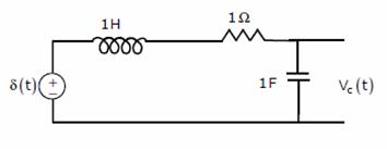
74. For t > 0, the output voltage Vc (t
) is
(A)  (B)
(B) 
(C) cos (D)
sin
(D)
sin
75. For t > 0, the voltage across the resistor
is
(A)  (B)
(B) 
(C)
sin (D) cos
Linked Answer
Questions: Q.76 to 85 Carry Two Marks Each
Statement
for Linked Answer Questions: 76 & 77
A two-port network shown below is excited by
external dc sources. The voltages and the currents are measured with voltmeters
V1, V2 and ammeter A1, A2 (all assumed
to be ideal), as indicated. Under following switch conditions, the readings
obtained are:
i) S1 - Open, S2 - Closed A1 = 0A, V1 = 4.5V, V2
= 1.5V, A2 = 1A
ii) S1 - Closed, S2 - Open A1 = 4A, V1
= 6V, V2 = 6V, A2 = 0A
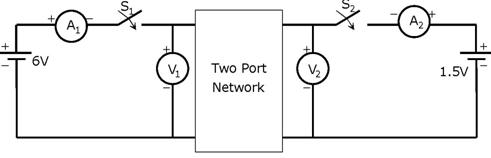
76. The z-parameter matrix for this network is
(A)  (B)
(B)  (C)
(C)  (D)
(D) 
77. The h-parameter matrix for this network is
(A)  (B)
(B)  (C)
(C)  (D)
(D) 
Statement for
Linked Answer Questions: 78 & 79
In the following network, the switch is
closed at t = 0- and the sampling starts from t = 0. The sampling frequency is
10Hz.
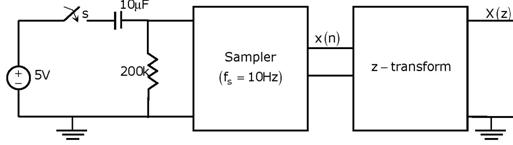
78. The samples x (n) (n = 0, 1, 2, ...) are
given by
(A) 5 (1 - e-0.05n) (B) 5e-0.05n (C) 5 (1 - e-5n) (D)
5e-5n
79. The expression and the region of convergence
of the z-transform of the sampled signal are
(A)  (B)
(B) 
(C)  (D)
(D) 
Statement for
Linked Answer Questions: 80 & 81
In the following transistor circuit VBE =
0.7V, rc = 25mV / IE, and b
and all the capacitances are very large
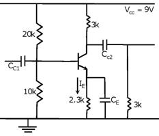
80. The value of DC current IE is
(A) 1mA (B) 2mA
(C) 5mA (D) 10mA
81. The mid-band voltage gain of the amplifier is
approximately
(A) -180 (B) -120
(C) -90 (D) -60
Statement for Linked Answer Questions: 82 & 83
In the following circuit, the comparator
output is logic "I" if V1 > V2 and is logic "0"
otherwise. The D/A conversion is done as per the relations
VDAC
=  volts,
where b3 (MSB), b2, b1 and b0 (LSB)
are the counter outputs the counter starts from the clear state
volts,
where b3 (MSB), b2, b1 and b0 (LSB)
are the counter outputs the counter starts from the clear state
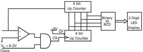
82. The stable reading of the LED display is
(A) 06 (B) 07
(C) 12 (D) 13
83. The magnitude of the error between VDAC
and Vin at steady state in volts is
(A) 0.2 (B) 0.3
(C) 0.5 (D) 1.0
Statement for
Linked Answer Questions: 84 & 85
The impulse response h(t) of a linear time
invariant continuous time system is given by h(t) = exp (-2t) u (t) , where u(t) denotes the unit step
function
84. The frequency response H(w) of this system in terms of angular
frequency w is given by H(w)
(A)  (B)
(B)  (C)
(C)  (D)
(D) 
85. The output of this system to the sinusoidal
input x (t) = 2cos (2t) for all time t, is
(A) 0 (B) 2-0.25 cos(2t - 0.125p)
(C) 2-0.5 cos(2t - 0.125p) (D) 2-0.5 cos(2t - 0.25p)
End of
Question Paper